


MOS420N10P Mosfet Module
Home Products SOT-227 Semiconductor DevicePower MOSFET moduleMOS420N10P Mosfet Module
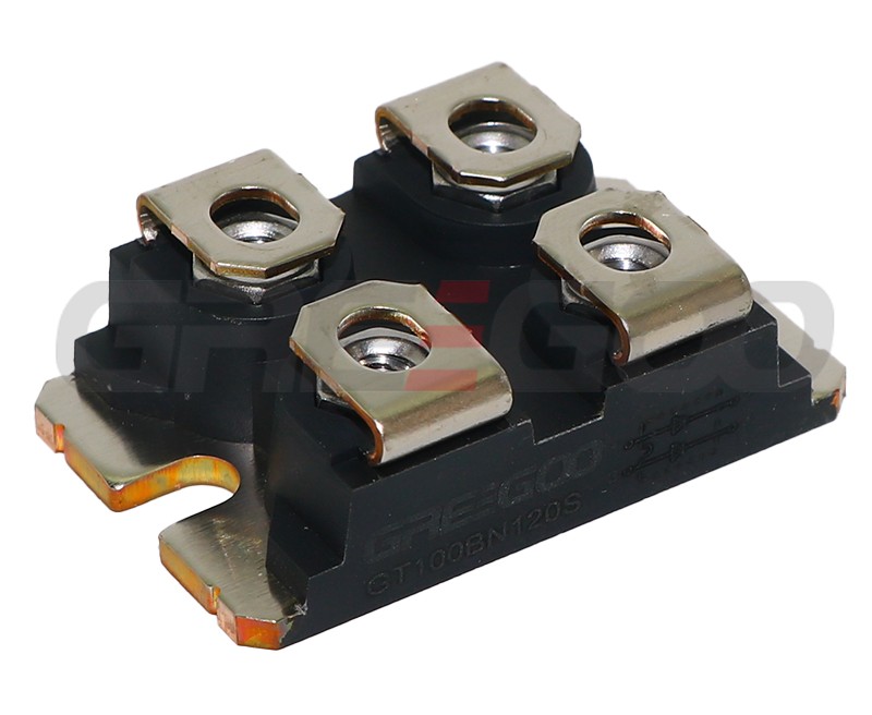
MOS420N10P Mosfet Module
Features:
- High power density
- Easy to mount
- Easy to use and parallel
- Fast intrinsic Rectifier
- Very short recovery time
- Isolation voltage 2500 VAC
- International standard package
Applications:
- DC-DC converters
- DC choppers
- Pulse generators
- Switched-mode and resonant-mode power supplies
Absolute Maxinmun Ratings
(Tc=25℃ unless otherwise specified)
|
Symbol |
Parameter |
Test Cobditions |
Value |
Units |
|
VDSS |
Drain-to-Source Voltage |
TJ = 25°C TJ =150°C |
100 |
V |
|
VGSS |
Gate-to-Source Voltage |
|
±20 |
V |
|
ID |
Continuous Drain Current |
TC=25 ℃ |
420 |
A |
|
IDM |
Pulsed Drain Current |
TC=25 ℃ |
1000 |
A |
|
EAS |
Single Pulse Avalanche Energy |
TC=25 ℃ |
4.2 |
J |
|
PD |
Maximum Power Dissipation ( TC=25 ℃) |
|
1100 |
W |
|
TJ |
Operating Junction Temperature Range |
|
-55 to 150 |
℃ |
|
TSTG |
Storage Temperature Range |
|
-55 to 150 |
℃ |
|
Visol |
Isolation Breakdown Voltage |
AC,50Hz,RMS,t=1min |
2500 |
V |
|
Torque |
Module to Sink |
M4 |
1.0-1.5 |
Nm |
|
Module Electrodes |
1.0-1.5 |
Nm |
||
|
Weight |
|
|
30 |
g |
|
Rthjc |
Junction to Case Thermal Resistance |
|
0.13 |
℃/w |
|
RthCK |
Case-to-Heat sink Thermal Resistance |
|
0.05 |
℃/w |
Electrical Characteristics (TC=25℃ unless otherwise noted )
|
Symbol |
Parameter |
Test Conditions |
Min. |
Typ. |
Max. |
Units |
|
BVDSS |
Drain-to-Source Breakdown Voltage |
VGS= 0V, ID= 250uA |
100 |
- |
- |
V |
|
IDSS |
Drain-to-Source Leakage Current |
VDS= 100V, VGS= 0V |
- |
- |
5 |
uA |
|
IGSS |
Gate-to-Source Leakage Current |
VGS=20V, VDS= 0V |
- |
- |
100 |
nA |
|
|
|
VGS= -20V, VDS= 0V |
- |
- |
-100 |
nA |
|
VGS(th) |
Gate Threshold Voltage |
VGS= VDS, ID= 250uA |
2.0 |
- |
4.0 |
V |
|
VRD(ON) |
Static Drain-to-Source On-Resistance
|
VGS=10V, IC=200A |
- |
- |
3.5 |
mΩ |
|
gfs
|
Forward Transconductance |
VDS=15V,ID=100A |
|
90 |
|
S |
|
Qg |
Total Gate Charge |
VDD=50V, ID=100A, VGS=10V
|
- |
242 |
|
nC |
|
Qgs |
Gate-to-Source Charge |
|
- |
60 |
|
nC |
|
Qgd |
Gate-to-Drain (Miller) Charge |
|
- |
135 |
|
nC |
|
t d(on) |
Turn-on Delay Time |
VDD=50V, ID=60A, VGS=10V Rg=3.3Ω |
- |
50 |
- |
ns |
|
t r |
Turn-on Rise Time |
|
- |
100 |
- |
ns |
|
t d(off) |
Turn-off Delay Time |
|
- |
110 |
- |
ns |
|
t f |
Turn-off Fall Time |
|
- |
230 |
- |
ns |
|
Ciss |
Input Capacitance |
VGS=0V, VDS=25V, f=1.0MHZ |
- |
50 |
- |
nF |
|
Coss |
Output Capacitance |
|
- |
4200 |
- |
pF |
|
Crss |
Reverse Transfer Capacitance |
|
- |
600 |
- |
pF |
Source-Drain Diode(TC=25℃ unless otherwise noted)
|
Symbol |
Parameter |
Test Conditions |
Min. |
Typ. |
Max. |
Units |
|
ISD |
Continuous Source Current
|
|
|
|
420 |
A |
|
ISM |
Pulsed Source Current |
|
|
|
1600 |
|
|
VSD |
Diode Forward Voltage |
IS=200A,VGS = 0V
|
- |
- |
1.5 |
V |
|
t r r |
Reverse Recovery Time |
VR = 50V IF= 25A, di/dt=100A/μs |
- |
150 |
|
ns |
|
I RM |
Diode peak Reverse Recovery Current |
|
- |
8 |
|
A |
|
Qr r |
Reverse Recovery Charge |
|
- |
0.48 |
|
uC |
Need more information?
Contact us to request pricing, availability and customization options.
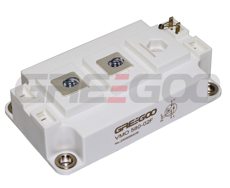
Power FET module VMO580-02F
HipPerFET Module VMO580-02F 200V 580A 3.8m N-Channel Enhancement mode
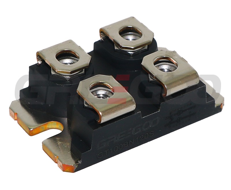
Silicon N-Channel Power MOSFET
The silicon N-channel Enhanced VDMOSFET is manufactured using self-aligned planar technology
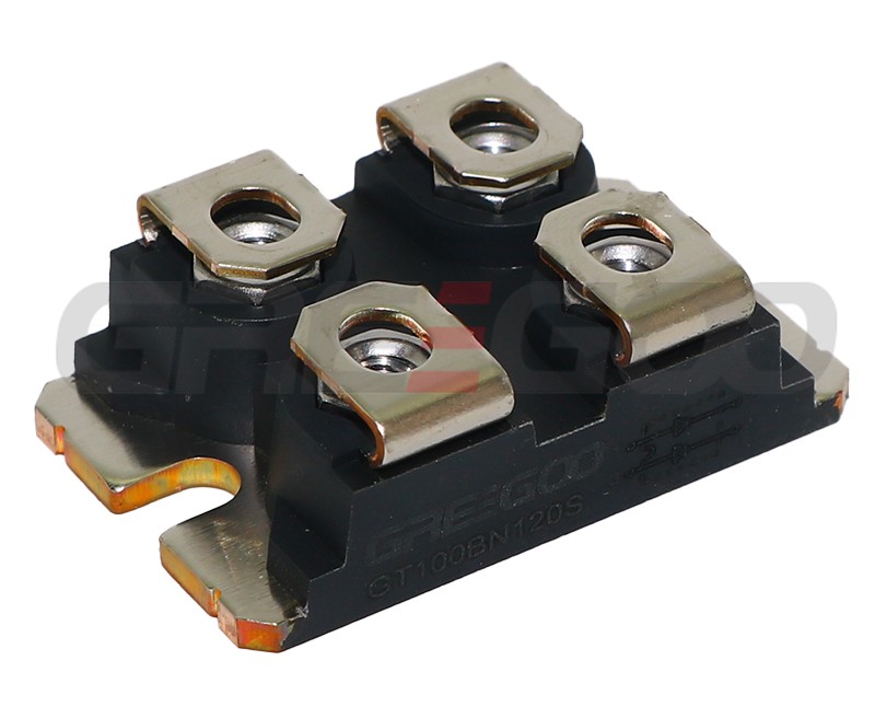
CAFN230N20 Silicon N-Channel Power MOSFET
210A 200V
CAFN50N120A Silicon N-Channel Power MOSFET
50A 1200V


We value your privacy
We use cookies to enhance your browsing experience, serve personalized ads or content, and analyze our traffic. By clicking "Accept All", you consent to our use of cookies.
